
HCLTech opens Bengaluru, Hubballi chip design centres for Japan's Rapidus
 By Pooja MehraIndustry Trends Analyst, Peepals Tech
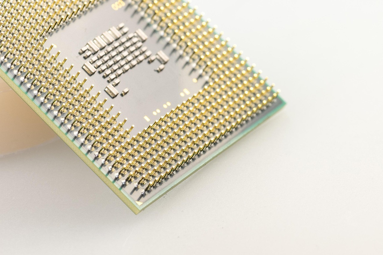
Representative image: blickpixel / Pixabay
HCLTech and Japan's Rapidus opened two chip engineering centres in Bengaluru and Hubballi on October 26, 2026, and plan an Indian talent pipeline.
What Happened
HCLTech, the Indian IT and engineering services company, and Rapidus Corporation, a Japanese company building advanced logic chips, opened two development centres in Karnataka on Monday, October 26, 2026, one in Bengaluru and one in Hubballi (also spelt Hubli). The two companies described the move as a partnership for next-generation semiconductor technologies. Engineers at the centres will handle several stages of chip design and design support for Rapidus, and HCLTech will also help Rapidus build a pipeline of Indian engineers for its work in Japan.
Key Facts
- Date and place: the centres in Bengaluru and Hubballi, Karnataka, were inaugurated on October 26, 2026.
- Work covered: mask design, design infrastructure, process design kit (PDK) development, design technology co-optimisation (DTCO) and layout design.
- Talent: HCLTech will work with Rapidus to develop Indian engineering talent for the Japanese company's changing needs in Japan.
- Rapidus view: CEO Atsuyoshi Koike said, "Through this collaboration with HCLTech, we expect to access India's growing pool of semiconductor engineering talent."
- Money: neither company disclosed the value or length of the contract.
- Location: one of the two centres is outside Bengaluru, in Hubballi, which spreads chip engineering work beyond the state capital.
Why It Matters
India's semiconductor story is often told through factories, but much of the value in a chip is created before any silicon is processed. The work listed for these centres sits in that early stage. Layout design turns a circuit into the physical pattern of transistors and wires. Masks are the stencils used to print those patterns onto a silicon wafer, so mask design must be exact. A process design kit is the rulebook and library that a chip company gives designers so their designs match what its factory can actually make. Design technology co-optimisation means tuning the design and the manufacturing process together so that the final chip is smaller, faster or uses less power. These are specialised skills, and a chipmaker that is still building up its operations needs many engineers who have them.
For Indian readers, the significance is twofold. First, it is a sign that Indian IT services firms are moving deeper into semiconductor engineering, a field with higher skill demands than routine software work. The companies say the centres will draw on HCLTech's core engineering experience. Second, the talent part of the deal points to Indian engineers supporting a Japanese chipmaker's own operations. Rapidus says the collaboration complements its work in Japan, so the link between the two countries here runs through companies and engineers rather than only through governments.
The choice of Hubballi is also worth noting. Most technology jobs in Karnataka cluster in Bengaluru. Placing a centre in a second-tier city gives local engineering graduates a chance at specialised work closer to home, though the reports did not say how many people the centres will employ.
| Term | What it means in plain words |
|---|---|
| Layout design | Drawing the physical arrangement of transistors and wiring on the chip |
| Mask design | Preparing the stencils that print the chip pattern on silicon |
| Process design kit | The factory's rulebook and building blocks for designers |
| Design technology co-optimisation | Tuning the chip design and the factory process together |
Impact
Short-term: The two centres begin providing design and engineering support to Rapidus. HCLTech gains a semiconductor client in Japan, although without a disclosed contract value its effect on the company's revenue cannot be judged.
Long-term: If the arrangement grows, it could build a base of Indian engineers trained in advanced chip design and manufacturing support, skills that India's own chip plans will also need. It may also encourage more foreign chip companies to place design work in Indian cities outside the main hubs.
Who is affected: Engineering graduates and chip designers in Karnataka, especially around Hubballi; HCLTech's engineering services business; Rapidus and its programme in Japan; and policymakers in both countries who are trying to grow their semiconductor industries.
Key Takeaway
HCLTech's new Bengaluru and Hubballi centres put Indian engineers to work on key design stages for Japan's Rapidus, a sign that Indian IT firms are moving into specialised chip engineering.
Questions and Answers
What did HCLTech and Rapidus announce on October 26, 2026?
They opened two development centres in Karnataka, in Bengaluru and Hubballi, as part of a partnership on next-generation semiconductor technologies. The centres will handle chip design and design-support work for Rapidus.
What work will the HCLTech centres do for Rapidus?
Mask design, design infrastructure, process design kit development, design technology co-optimisation and layout design. In short, they cover the steps that turn a chip design into patterns a factory can manufacture.
Will Indian engineers work for Rapidus in Japan?
HCLTech says it will work with Rapidus to build a pipeline of Indian engineering talent to meet the Japanese company's needs in Japan. The companies did not give numbers or a timeline.
How much is the HCLTech-Rapidus deal worth?
The value and duration of the contract were not disclosed by either company.
Disclaimer: Prepared by the Peepals newsroom from publicly available sources with AI assistance. Information is accurate to the best of our knowledge at the time of publication and may change. Images may be representative. Not professional advice. Report an error via our contact page.
By Pooja Mehra, Industry Trends AnalystCovers Industry News & Trends and more for Peepals Tech. All stories by Pooja Mehra
New iPad mini 2026 gets OLED and A20 Pro, priced Rs 82,900
OpenAI says its AI disproved the Exponential Time Hypothesis; experts to check
Get the day's stories in your inbox
Peepals Weekly: the week decoded, free. One email a week, unsubscribe in one click.
Pooja Mehra is a pen name of the Peepals Global Editorial Team, which researches, fact-checks and publishes every story. The portrait is an illustration.